

One thing I’ve learned from ordering PCBs is that more area usually means more cost. If I were to make a single circular PCB with a big gaping hole in the center, that would be an enormous waste of money.
Instead, I decided to break the buttons into individual modules. (Turns out modular systems are kind of my thing.) Each module uses the same PCB design, but at the same time, it can function as a standalone button.
We don’t need a microcontroller for every button—that would be complete overkill. Instead, I designed a “bus station” that all the modules share. This bus allows buttons 2–8 to route their signals back to the main module, which contains the microcontroller. Button 1 is connected directly to the main module by default.
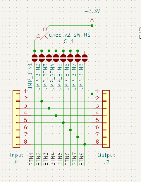
Each module has pads that can be shorted by the user. These pads are all connected to the same button within that module, but what changes is which port the signal is routed to.
Each pad corresponds to a specific button pin. By shorting certain pads, the user can control where the button signal travels along the bus, effectively routing it to the desired module.
Think of it like train tracks: the user decides which path the signal takes, and the signal follows the track to the microcontroller.
With this modular design, we can create multiple button modules without blowing the budget.
Bonus points: most PCB manufacturers produce boards in sets of five. That means I can order 10 copies of the PCB and actually use 8 of them without expensive leftover scraps collecting dust.
Update: Or that was the idea... till I realized that I kind messed up and used the wrong footprint for the micro controller. Happens... I had to buy another batch with the correct sizing